The Hidden Gap That Could Break Moore's Law—And the Global Race to Close It
BEIJING — May 2026 – For half a century, the semiconductor industry has been governed by a single, relentless principle: make the transistor smaller, and everything gets better. Smaller transistors switch faster, consume less power, and pack more densely onto a chip. Moore's Law, the observation that transistor density doubles roughly every two years, has been the drumbeat of progress, and the industry has marched to it with extraordinary discipline.
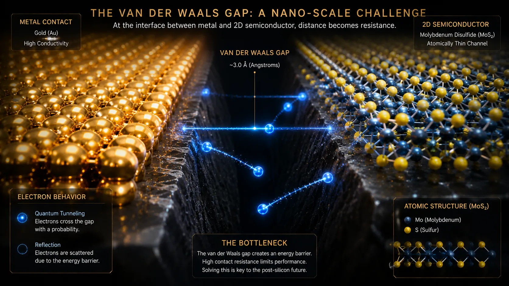
But at the atomic scale, the rules change. In the emerging world of two-dimensional semiconductors—materials like molybdenum disulfide that are literally a few atoms thick—the industry has collided with a problem that no amount of process refinement can solve. When you lay a metal contact on a 2D semiconductor, the two materials do not bond. They sit next to each other, separated by a gap—a van der Waals gap—that is only a few angstroms wide but acts as a formidable tunneling barrier. Electrons must quantum-mechanically tunnel through this gap to enter or leave the semiconductor, and the resulting contact resistance degrades performance in ways that threaten to halt the miniaturization of logic devices entirely.
In 2026, the race to close the gap has become one of the most urgent and competitive research frontiers in the global semiconductor industry. Breakthroughs are emerging from China, the United States, and Europe, each offering a different approach to a problem that may determine whether the post-silicon era delivers on its promise—or stalls before it begins.
The Gap That Should Not Exist
The van der Waals gap is not a defect. It is a consequence of physics. Two-dimensional materials like transition metal dichalcogenides have surfaces that are chemically inert. There are no dangling bonds, no reactive sites where a metal contact can form a strong chemical connection. When metal is deposited on top, the interface is held together only by van der Waals forces—the weakest of all intermolecular interactions. The result is a physical separation that electrons must cross by tunneling, and tunneling is inherently inefficient.
This problem has been understood for years, but it has become urgent as the semiconductor industry approaches the limits of silicon scaling. 2D semiconductors are widely regarded as the most promising channel materials for ultimately scaled transistors, offering superior electrostatic control at sub-nanometer thicknesses. But a transistor is only as good as its contacts. If the contact resistance cannot be reduced to levels comparable to silicon, the performance advantages of 2D channels will remain theoretical.
A January 2026 paper in Nature Communications demonstrated one approach: using metallic tellurium evaporated onto molybdenum ditelluride to form an atomically sharp van der Waals gap with optimal band alignment. The tellurium-based contact achieved efficient p-type carrier injection, addressing a long-standing asymmetry in 2D transistor development.
A more radical solution emerged from China's National Center for Nanoscience and Technology, where researchers proposed a new contact strategy called atomic-layer bonding. Their work, published in the Journal of Semiconductors in February 2026, achieved an ultra-low contact resistance of 70 Ω·μm, combined with 400°C thermomechanical stability and a high on-state current of 1.1 mA/μm. These are silicon-class numbers, achieved on a 2D platform, and they represent a paradigm shift in contact engineering.
The Global Stakes
The race to close the van der Waals gap is not merely academic. It is a competition with profound economic and geopolitical implications. The company or country that solves the contact resistance problem for 2D semiconductors will have a decisive advantage in the next generation of logic chips—the chips that will power AI inference engines, edge computing devices, and the vast array of sensors and processors that will define the post-smartphone era.
TSMC, the world's largest contract chipmaker, has been quietly investing in 2D materials research for years. In 2024, the company demonstrated a 2D semiconductor transistor with a gate length of just 1 nanometer, suggesting that the material platform is viable for production. But the contact resistance problem remains the bottleneck. Without a manufacturable solution, the 1-nanometer gate is a laboratory curiosity.
The Chinese government has identified 2D materials as a strategic research priority, funding multiple national laboratories through its 14th Five-Year Plan. The European Union's Graphene Flagship has expanded its scope to include other 2D materials, including transition metal dichalcogenides. The United States, through the CHIPS Act and the National Semiconductor Technology Center, is funding 2D materials research as part of its broader effort to maintain leadership in advanced semiconductor technology.

What Every Entrepreneur Can Learn
The van der Waals gap problem offers lessons for anyone building at the frontiers of technology.
First, the interface is often more important than the component. The semiconductor industry has spent decades optimizing the transistor channel, but the performance bottleneck has shifted to the contacts—the interface between the channel and the outside world. This pattern repeats across technology: the battery-electrode interface determines battery life, the implant-tissue interface determines biocompatibility, the user-software interface determines product adoption. The entrepreneurs who focus on interfaces rather than components often find the largest unsolved problems.
Second, a fundamental physics problem is a business opportunity. The van der Waals gap is not something that can be resolved through incremental process improvement. It requires a fundamental innovation in how materials are joined at the atomic scale. The companies that develop and patent those innovations will own a critical piece of the semiconductor supply chain for decades.
Third, the post-silicon transition is not a single event. It is a cascade of interconnected problems—contact resistance, dielectric integration, thermal management, manufacturability—each of which represents a potential company. The entrepreneurs who break the transition into its constituent bottlenecks and solve one of them exceptionally well will be rewarded, even if they never touch a transistor channel.
The Road Ahead
The van der Waals gap will not close overnight. The solutions emerging from laboratories in Beijing, Dresden, and Cambridge are promising, but they must be integrated into manufacturing processes that can produce billions of transistors with acceptable yield and cost. The semiconductor industry moves slowly, even when it moves urgently, and the transition from silicon to 2D materials will be measured in decades, not years.
But the direction of travel is unmistakable. The contact resistance problem has been identified, characterized, and now—through atomic-layer bonding, metallic tellurium contacts, and a growing family of interface engineering techniques—is beginning to yield. The gap that threatened to halt Moore's Law may yet be bridged. And when it is, the companies that own the bridging technology will have a claim on one of the most valuable pieces of industrial real estate on Earth.