
The ₹91,000 Crore Silicon Dream: Tata's Dholera Fab Goes Live—And India Finally Has a Semiconductor Footprint the World Can't Ignore
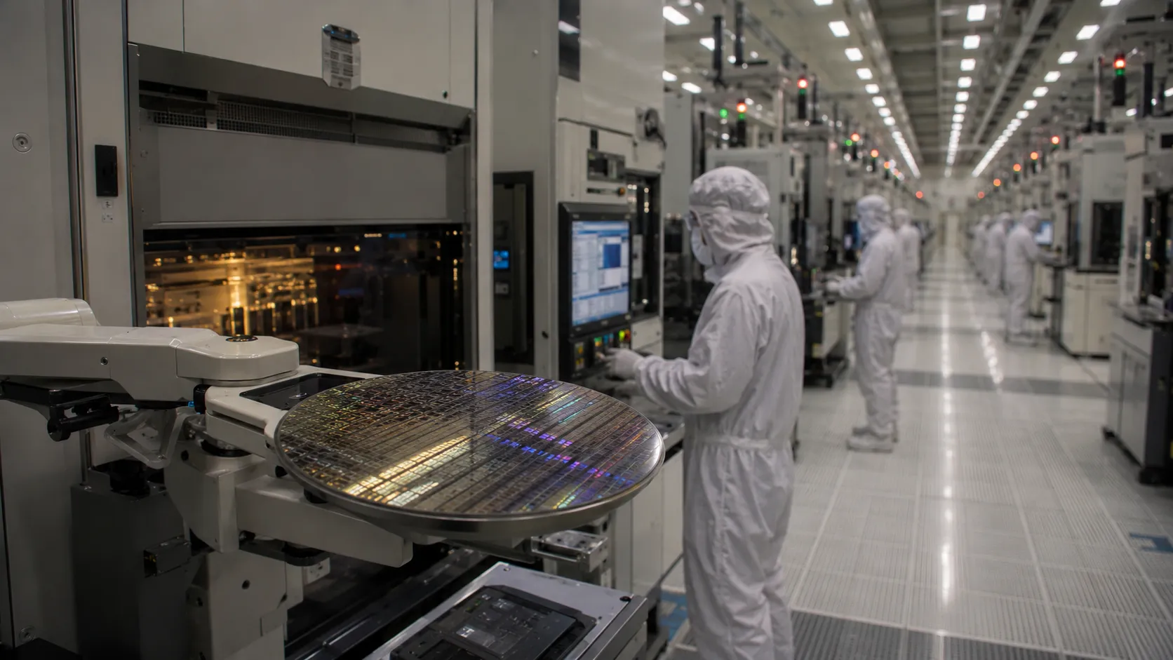
DHOLERA, GUJARAT — May 30, 2026 — On a Tuesday morning three weeks ago, in a hermetically sealed cleanroom on a 1,200‑acre campus in Gujarat's Dholera Special Investment Region, a robotic arm lifted a 300‑millimetre silicon wafer from a sealed pod and placed it into a lithography machine. The machine—a deep‑ultraviolet scanner, manufactured by ASML and imported from the Netherlands under the technology‑transfer agreement that had taken four years to negotiate—etched the first patterns onto the wafer's surface. The wafer moved through a series of processing stations: deposition, etching, ion implantation, chemical‑mechanical planarisation. Forty‑eight hours later, it emerged as a finished 28‑nanometre chip—the first semiconductor ever manufactured on Indian soil by a commercial fabrication plant. The chip was not cutting‑edge by the standards of TSMC's 3‑nanometre process, but it did not need to be. It was a proof of concept: India, which had spent decades trying and failing to build a domestic semiconductor industry, could finally make a chip.
The Dholera plant, built by Tata Electronics in partnership with Taiwan's Powerchip Semiconductor Manufacturing Corporation, is the first of three commercial fabs that are being developed under the Indian government's ₹76,000 crore India Semiconductor Mission. The plant's total cost—₹91,000 crore, including the government's capital subsidy—makes it the single largest private‑sector investment in Indian manufacturing history. Its initial production capacity is approximately 50,000 wafers per month, a figure that is modest by global standards but that represents a starting point from which the plant can scale. The second fab, being built by Tata in partnership with TSMC in Assam, is designed for 22‑nanometre production and is expected to begin operations in 2028. The third, a packaging and testing facility being built by Micron in Gujarat, is already operational. Together, the three facilities represent the foundation of an Indian semiconductor ecosystem that the country's policymakers have been pursuing for half a century—and that has, until now, remained stubbornly out of reach.
The Fifty‑Year Gap
The most important context for the Dholera fab is the fifty‑year gap that preceded it. India's attempts to build a semiconductor industry date back to the 1970s, when the government established the Semiconductor Complex Limited in Mohali—a state‑owned enterprise that was supposed to produce India's first indigenous chips. The SCL failed, as did every subsequent attempt. The reasons were consistent across the decades: underinvestment, bureaucratic mismanagement, the absence of a domestic electronics manufacturing ecosystem to create demand for the chips, and the simple, brutal reality that the global semiconductor industry was consolidating around a handful of giant players—TSMC in Taiwan, Samsung in South Korea, Intel in the United States—whose scale, technology, and capital advantages made it virtually impossible for a new entrant to compete.
The fifty‑year gap created a structural vulnerability that the Indian government has, in recent years, come to recognise as a national‑security imperative. India imports virtually all of its semiconductors—approximately $25 billion worth annually—from a global supply chain that is concentrated in a handful of geopolitically sensitive locations. The chips that power India's smartphones, its electric vehicles, its defence systems, and its industrial infrastructure are almost entirely manufactured abroad, and the supply chain that delivers them is vulnerable to the same disruptions—natural disasters, geopolitical conflicts, trade restrictions—that have reshaped the global semiconductor industry over the past decade. The COVID‑19 pandemic, the U.S.‑China technology war, and the Russian invasion of Ukraine each exposed a different dimension of that vulnerability, and each reinforced the urgency of building a domestic chip‑manufacturing capability.
The India Semiconductor Mission, launched in 2022 with an initial outlay of ₹76,000 crore, was the government's response to that vulnerability. The ISM's structure—a combination of capital subsidies, infrastructure support, and technology‑transfer facilitation—was modelled on the successful semiconductor policies of Taiwan, South Korea, and Israel, each of which had used government intervention to build a domestic chip industry from scratch. The ISM's architects understood that the market alone would not deliver a semiconductor fab to India—the barriers to entry were too high, the capital requirements too large, and the returns too uncertain to attract private investment without government support. The government's role was to absorb the initial risk, to provide the infrastructure and the incentives that would make the investment viable, and to signal to the global semiconductor industry that India was serious about building a domestic manufacturing base.
The Tata‑PSMC partnership was the first major agreement to emerge from the ISM framework, and its terms reflect the government's willingness to invest in semiconductor manufacturing at a scale that no previous Indian administration had attempted. The government is providing approximately 50 percent of the Dholera fab's capital cost through a combination of direct subsidies, tax incentives, and infrastructure support, while Tata is contributing the remaining capital and PSMC is providing the technology transfer and the operational expertise. The partnership is structured to ensure that the technology, the intellectual property, and the manufacturing know‑how are transferred to Tata over time, reducing India's dependence on foreign partners as the domestic semiconductor ecosystem matures. The model is borrowed from the Taiwanese experience—the government provides the capital and the infrastructure, the foreign partner provides the technology, and the domestic company gradually absorbs the capability and builds its own independent manufacturing base.
The Mature‑Node Strategy
The most strategically significant dimension of the Dholera fab is not the fact that it exists. It is the node at which it operates. The 28‑nanometre process that the fab is using is, by the standards of the global semiconductor industry, a mature technology. TSMC and Samsung are manufacturing at 3 nanometres, and their 2‑nanometre processes are in development. The 28‑nanometre node, which was first commercialised in the early 2010s, is two or three generations behind the cutting edge. The global chip industry's attention is focused on the race to ever‑smaller geometries—the angstrom‑level precision that enables the most advanced processors, the most powerful AI accelerators, and the fastest smartphones. The 28‑nanometre chip that the Dholera fab is producing is not, by those standards, impressive.
The mature‑node strategy is not a compromise. It is a deliberate choice, driven by the structure of the Indian semiconductor market. The chips that India consumes in the largest volumes are not the cutting‑edge processors that power the latest smartphones or the most advanced AI servers. They are the mature‑node chips that go into smart meters, electric‑vehicle battery controllers, industrial sensors, medical devices, and the growing array of connected devices that are being deployed across India's infrastructure. These chips do not require the most advanced manufacturing technology. They require reliability, low cost, and a supply chain that is not vulnerable to geopolitical disruption. The 28‑nanometre node, which is both mature and capable enough to serve the vast majority of India's chip demand, is the optimal entry point for a domestic semiconductor industry. It is the node that can build the volumes, the yields, and the manufacturing expertise that are the prerequisites for eventually moving to more advanced nodes. It is a starting point, not a destination, and the trajectory from 28 nanometres to 22 nanometres to 14 nanometres is the trajectory that every successful semiconductor industry has followed.
The mature‑node strategy also aligns with the global restructuring of the semiconductor supply chain. The U.S.‑China technology war has made it increasingly difficult for Chinese manufacturers to export mature‑node chips to global markets—a disruption that has created an opportunity for Indian manufacturers to capture a share of the global mature‑node market. The Dholera fab's initial production is being sold primarily to Indian customers, but the plant's capacity can be scaled to serve export markets in Southeast Asia, Africa, and the Middle East—markets that are experiencing the same growth in demand for mature‑node chips that India is, and that are looking for reliable, geopolitically neutral suppliers. The mature‑node strategy is, in this sense, not merely a domestic‑market play. It is a global‑market play, and the market is large enough to support multiple suppliers. The Indian semiconductor industry's entry point is not the cutting edge, but the foundation—the chips that power the everyday electronics that the world consumes in the billions of units. The foundation is less glamorous than the frontier, but it is larger, more stable, and more accessible to a new entrant. The Dholera fab's 28‑nanometre chip is the first step on a ladder that extends, eventually, to the cutting edge—and the ladder has been climbed, step by step, by every country that has ever built a semiconductor industry.
The Ecosystem Gap
The most significant challenge facing the Dholera fab is not the technology. It is the ecosystem. A semiconductor fabrication plant does not exist in isolation. It exists within a dense network of suppliers, service providers, and customers—the specialty chemical companies that provide the high‑purity gases and solvents, the equipment manufacturers that provide the deposition and etching tools, the packaging and testing companies that turn the finished wafer into a usable chip, and the electronics manufacturers that buy the chips and integrate them into products. The ecosystem that surrounds a semiconductor fab is as important as the fab itself, and the ecosystem in India is, at present, thin.
The Indian government is aware of the ecosystem gap and is attempting to fill it through the same combination of incentives and infrastructure that made the Dholera fab possible. The ISM's framework includes provisions for the development of a semiconductor supply chain—incentives for the specialty chemical companies, the equipment manufacturers, and the packaging and testing companies that are essential to a functioning semiconductor industry. The government has also been negotiating with global semiconductor equipment manufacturers—Applied Materials, Lam Research, Tokyo Electron—to establish service centres in India that can support the fabs that are being built. The ecosystem is being constructed alongside the fabs, but it will take years to mature—and the fabs that are already operational will depend, in the interim, on imported chemicals, imported equipment, and imported services that reduce their cost competitiveness. The ecosystem gap is the single most important variable in the Indian semiconductor industry's development, and closing it will require sustained investment over a decade or more.
The ecosystem challenge is compounded by the talent gap. The semiconductor industry requires a highly specialised workforce—process engineers, equipment technicians, materials scientists—that does not exist in India at the scale that the fabs will require. The Dholera plant's initial workforce of approximately 3,000 engineers and technicians was recruited, in significant part, from the Indian diaspora—engineers who had been trained at Intel, TSMC, and Samsung, and who returned to India to participate in the domestic semiconductor industry's launch. The next generation of Indian semiconductor engineers is being trained at the Indian Institutes of Technology, the Indian Institute of Science, and a growing number of specialised semiconductor‑training programmes that are being established in partnership with the industry. The talent pipeline is being built, but it will take years to mature—and the fabs that are being built today will depend, in the interim, on a workforce that is being recruited from abroad and repatriated at considerable cost. The talent gap is the most binding constraint on the Indian semiconductor industry's growth, and closing it is a generational project.
The Geopolitics of the Chip
The Dholera fab is not merely an industrial project. It is a geopolitical statement. The global semiconductor industry is the most strategically contested sector of the 21st‑century economy—the foundation on which everything from artificial intelligence to autonomous weapons is built. The countries that control the most advanced chip‑manufacturing capabilities—Taiwan, South Korea, the United States, and, increasingly, China—control the technological future. The countries that do not are dependent on the countries that do, and that dependence is a structural vulnerability that no amount of diplomatic alignment can fully mitigate.
The Indian government's decision to invest ₹76,000 crore in domestic semiconductor manufacturing is a recognition of that vulnerability. India cannot afford to depend on Taiwan, or South Korea, or China, or the United States for the chips that power its economy, its military, and its infrastructure. The Dholera fab is the first step toward a sovereign semiconductor capability—a manufacturing base that is owned by an Indian company, operated by Indian engineers, and integrated into the Indian electronics manufacturing ecosystem. The capability is modest, at present, but it will grow over time, and the growth will be driven by the same strategic imperative that has driven every other country that has built a semiconductor industry: the recognition that the chips that power a nation's future must, ultimately, be made within its own borders.
The geopolitical context also shapes the Dholera fab's commercial prospects. The U.S.‑China technology war has disrupted the global semiconductor supply chain, and the disruption has created opportunities for new entrants to capture market share from the incumbents. The mature‑node chips that the Dholera fab is producing are the same chips that Chinese manufacturers have historically supplied to global markets—and that global customers are increasingly reluctant to source from China, given the geopolitical risks. The Indian fab that can offer a reliable, geopolitically neutral alternative to Chinese mature‑node chips has a market that extends well beyond India's borders, and the Dholera fab's initial production is already being sold to customers in Southeast Asia, the Middle East, and Africa. The geopolitics of the chip is, in this sense, both the problem and the opportunity. It is the problem that made the Dholera fab necessary, and it is the opportunity that will make it commercially viable.
What This Signals
The Dholera fab is not primarily a story about a factory. It is a story about the structural transformation of the Indian economy—a shift from an economy that consumes technology to an economy that produces it, from a market that is dependent on global supply chains to a market that is building its own, and from a nation that was once content to be a spectator in the semiconductor industry to a nation that is determined to be a participant. The transformation will take decades, and it will require sustained investment, sustained political will, and sustained patience from the companies and the engineers who are building the industry from scratch. The Dholera fab is the first step on that journey. The chip that rolled off its line three weeks ago is a modest artefact, a 28‑nanometre circuit that is two generations behind the cutting edge. But it is, for the first time, an Indian artefact—a chip that was made in India, by Indian engineers, on Indian soil. The fifty‑year gap is closed. The next fifty years have begun.